投稿

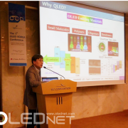
[Lighting Japan 2016] What is the Key Issue of Solution OLED Materials?

In Lighting Japan 2016 (January 13-16) conference, Sumitomo Chemical and Merck revealed recently developed soluble OLED materials performance results.


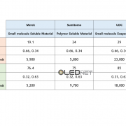
The soluble OLED materials efficiency published in this conference reached ≥ 65% of UDC’s evaporation materials; particularly, Sumitomo Chemical’s red achieved ≥ 85%, and green reached ≥ 88% of UDC’s evaporation materials efficiency. Lifetime (LT 95) results were not as good as efficiency with red’s 25% and green’s approximately 40% (average).


Sumitomo Chemical and Merck both revealed that although in terms of efficiency the soluble materials almost caught up to evaporation materials, but lifetime requires further development.


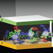
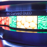
Solution process is a method that allows for large area OLED panel production in RGB method using ≥ Gen8 manufacturing equipment. Key panel companies are actively carrying out research development, and the performance of soluble OLED material is considered the biggest issue. According to Solution Process OLED Report 2015, published by UBI Research, when solution process is applied the material cost can be approximately 40% reduced compared to the current evaporation process using large area OLED panel. The timing for the solution process application to mass production is expected to be decided depending on the development speed of soluble OLED materials.


OLED Materials Performance Comparison

OLED Materials Performance Comparison

New Solution for Next Generation OLED Lighting

Professor Lee Taek Seung of Chungnam National University

Professor Lee Taek Seung of Chungnam National University


Professor Taek Seung Lee and Jongho Kim (Chungnam National University’s Department of Advanced Organic Materials and Textile System Engineering), and Professor Jin Sung-Ho and Park Juhyeon (Pusan National University’s Graduate Department of Chemical Materials, and Institute for Plastic Information and Energy Materials) authored a paper titled ‘Synthesis of conjugated, hyperbranched copolymers for tunable multicolor emissions in light-emitting diodes’. For 2015 June issue, Polymer Chemistry, published by the Royal Society of Chemistry, selected it as its back cover.


The paper discusses research of polymer material applied to solution process and explains that through polymer structure in the form of hyperbranched red, green, and blue monomers, diverse colors, including white, can be actualized depending on the amount of each monomer. Existing OLED lighting used R/G/B or YG/B stacking structure to produce white OLED, complicating the process. Although a method of producing white by combining R/G/B together is being developed, energy displacement between R/G/B can cause unwanted colors. However, if the R/G/B monomers can be introduced to polymer structure as hyperbranched forms as the paper suggests, the energy displacement can be minimized when the polymer solidifies which makes it easier for the colors to be realized.


Professor Lee revealed that hyperbranched polymer materials were used in the research and that as white can be produced from just one polymer material, simple process can be used for the production.


The patent for this technology has been applied (application number 10-2012-0091350) in Korea. It is anticipated that this will become a key technology for reducing the next generation OLED lighting production cost.


원리

Large Size OLED Panel Technology Match, ‘WRGB vs. Solution Process RGB’

Large size OLED panel is currently being mass produced by LG Display using WRGB method, and investment in this method for large size panel is being considered by OLED panel latecomers. Another method that can be used to produce OLED is RGB method. In 2013 Samsung Display mass produced using RGB method but halted the process due to problems in yield rate and technology. However, recently as key display companies are developing RGB method using solution process for large area OLED panel, latecomers are having to make a difficult choice in process selection.


OLED specialized panel company JOLED, established by JDI, Sony, Panasonic, and Innovation Network Corporation of Japan (INCJ), is aiming for mid-to-large size OLED panel production using solution process. Additionally, other companies including AUO, BOE, LG Display, and Samsung Display are developing large size OLED panel using solution process technology. In 2013, AUO presented 65 inch FHD panel that used solution process technology, and BOE revealed 30.5 inch FHD panel. Panasonic also presented solution process applied 4K panel.


According to 2015 White OLED Display Annual Report, published by UBI Research, WRGB method has an advantage in high mass production potential as open mask is used. However, due to the stack structure and color filter use, it has a disadvantage of increased panel production cost. On the other hand, the materials and process technology for solution process are not yet mature, but has the advantage of being able to produce large size OLED panel in Gen 8 size or larger without glass cutting using RGB method. It also can reduce the production cost as the material efficiency is high and does not require color filter.


At present the mass produced glass area by the latecomers forecast to manufacture large area AMOLED panel is expected to occupy approximately 30% of the total large area OLED market in 2020, and latecomers’ choice in technology investment will be a key point. Therefore, the large area panel technology leadership will be decided on whether WRGB and solution process methods can solve the issues that each has.

By DaRae Kim, reporter@olednet.co.kr

JOLED’s Intense Start, Mass Production is When?

At Finetech Japan 2015 (April 8-11, 2015), JOLED gave a presentation for the first time since its inception and drew much attention.


JOLED’s speaker Tadashi ISHIBASHI gave a presentation on JOLED’s target market and application technology under the title of “The Evolution of OLED Manufacturing Technology by JOLED”. During his speech Ishibashi revealed “JOLED’s target market is 10~30 inch mid-size OLED panel and ultimately to form new market through flexible display” and that “top emission, RGB printing, color filter, and ITZO backplane of self-align structure will be applied for key technology”.


Furthermore, by forming all RGB through solution process, macro-cavity effect via thin half-transparent cathode, and minimizing interference of other colors and external reflection using color filter, JOLED explained that high purity color reproduction is possible. It is analyzed that this means that they absorbed Sony’s characteristic super top emission technology. Backplane is top-gate’s TAOS (transparent amorphous oxide semiconductor) and Ishibashi added that it is also possible to reduce cost by minimizing investment amount by applying 5 mask self-align structure.


Regarding flexible display, JOLED used the technology that was applied to 9.9 inch qHD panel (revealed by Sony in 2012) which used white OLED and color filter as an example but reported they are currently developing technology to produce flexible display using solution process RGB.


From the presentation it is estimated that for JOLED’s mass production, Sony’s OLED panel structure and Panasonic’s RGB printing technology will be combined and applied. Although detailed investment timeline was not revealed, as mass production application technology and target have been publicly announced, investment in near future is anticipated.

150415_본격적인 행보를 시작한 JOLED, 양산 시점은

150415_본격적인 행보를 시작한 JOLED, 양산 시점은1

Prof. Changhee Lee of Seoul National University, ‘Anticipate QLED’s Future’

Professor Changhee Lee of Seoul National University discussed QLED’s future in the 1st OLED KOREA Conference (April 2), organized by UBI Research.


QLED is a display that replaced emitting layer’s host and dopant to quantum dot (QD) whilst continuing to use existing OLED’s common layer, and can be formed via solution process. It can be mistaken as similar concept with recently released quantum dot products. However, these are devices that have quantum dot film attached to LCD and therefore fundamentally different from QLED which has basis on OLED.


Of the OLED panel cost, the expensive OLED key emitting layer materials, host and dopant, take up a high percentage. On the other hand, OLED’s emitting material quantum dot uses inorganic material which is cheaper compared to OLED material. This means that the QLED panel can be more reasonably priced, a point of great interest for the industry.


However, in order for QLED to be practical there are several issues that need to be solved. Balancing the electrons and holes, and prevention of pin holes that occur in each layer is a key technology needed to increase QLED’s efficiency that is quickly being developed. Also, although cadmium used in QLED is not likely to affect the environment, considering future environmental regulatory concerns quantum dot without cadmium is being researched. Lastly, solution process technology has to be established.


If QLED overcomes these issues and its lifetime and efficiency can match those of existing OLED, it is estimated QLED applied products will be manufactured. Professor Lee forecast that QLED would bring positive results of bringing down the cost of display while maintaining most of existing OLED process; QLED uses cheaper quantum dot material for emitting layer whilst continuing to use equipment and common layer of existing OLED technology. Additionally, he also concluded that there will not be any problem for material companies as they will be able to carry on selling materials for quantum dot. Professor Lee went on to ask OLED related companies with anti-QLED views to accept QLED in the same flow as OLED, and for positive considerations.


Prof. Changhee Lee, the 1st OLED KOREA Conference

Prof. Changhee Lee, the 1st OLED KOREA Conference

Solution-processed OLED to be commercialized in years

A solution-processable OLED technology is the one of its kinds that can RGB panels by using mother glasses for Gen 6 or later OLED panels. After some improvements are made to the properties of materials and definition, solution-processed OLED products will be manufactures in years to come.


So far, the existing solution process technology with a resolution of 200ppi could not be applied to smartphones and tablet PCs requiring a higher definition. With the development of the new technology that can feature a resolution of up to 300ppi, however, the solution process can become applied to tablet PCs with the potential for rapid growth.


In addition, it is possible that solution process technology is utilized to manufacture ultra HD 4K and even 8K (7680×4320) TV panels. The 65-inch 8K (7680×4320) panels are expected to feature a resolution of approximately 140 ppi. The manufacturing of panels that can produce an image of 200 ppi or higher will lead to the production of high-definition RGB LED TV panels.


Given that the 10.5-inch panels using the recently released AMOLED panels have a resolution of 287 ppi and use a Pentile layout, tablet PC panels with a RGB layout will be manufactured by using the solution process technology.

Portfolio Items