投稿

JOLED、Solution Process OLED後工程の量産ライン構築開始

JOLEDが中型サイズのSolution Process OLED量産のため後工程ラインを千葉事業所に構築すると発表した。 JOLEDのSolution Process OLEDは路尾事業所からTFT工程から印刷工程までである”全工程”が進んだ後、千葉事業所でモジュール工程と最終検査まで行われる”後工程”が実施される。

JOLEDは月22万台の生産量を目標にしており、2020年に千葉事業所と能美事業所を同時に稼動する計画だ。

JOLEDのSolution Process OLEDは、自動車とハイエンドのモニター市場をターゲットとしており、大きさは10~32型範囲である。

一方、JOLEDは2018年12月5日から7日まで日本の東京で開かれた28th FINETECH JAPANでe-sports用と医療分野用専門21.6型FHD OLEDモニター、自動車用12.3型HD OLEDと12.2型FHD flexible OLEDなど多様な中型の大きさのSolution Process OLEDを披露した。

ASUS-最初のsolution process OLED商用化モニターの『PQ22UC』販売開始

ASUSがJOLEDのsolution process OLEDが適用されたモニターである『PQ22UC』をオーストラリアと英国で販売を開始する。

<Asusの『PQ22UC』, Source: asus.com>

2018年に開かれた〝CES 2018”で公開された『PQ22UC』は、最初に商用化されたsolution process OLEDモニターという点で多くの注目を受けた。

『PQ22UC』の大きさは21.6型で、解像度は4K(204ppi)、輝度は140 nit/330 nit(一般/最大)、応答時間は0.1 ms、コントラスト比は1,000,000:1だ。

また、折り畳み式スタンドと折りたたみ式保護ケースが提供され、1kg未満の重さによって簡単に携帯が可能であるという長所がある。 このようなメリットにより外部で写真作業や映像撮影など専門的な作業を主に手がけるユーザーにも役立つものと見られる。

現在英国とオーストラリアのセレクトショップ(select shop)での価格は税込みそれぞれ£4,699と€5,160水準だ。 モバイル機器やテレビでシェアを拡大しているOLEDがモニター市場でもシェアを拡大していけるかどうかが注目される。

プレミアムTV市場をリードする 大面積OLEDへの投資額は?

■ WRGB OLEDとソリューションプロセスOLED、QD-OLEDへの投資額を比較分析
■ 2018年から2022年までのOLED製造装置市場は588億米ドル、検査装置市場は84億米ドル規模になる見込み

最近、プレミアムTV市場ではOLED TVのシェアが拡大を続けている。OLED TVは、WRGB OLEDにカラーフィルターを採用した構造で、現在は唯一LG DisplayがOLEDパネルを量産している。

そこで、Samsung DisplayはプレミアムTV市場でWRGB OLEDに対抗するために「青色OLED + 量子ドットカラーフィルタ(Quantum Dot Color Filter、QDCF)」を開発していると知られている。青色OLEDはOLEDから発される青色光が量子ドット層とカラーフィルターを通り抜け、赤色と緑色を実現する技術である。


<QD-OLED構造の予測>

UBI Researchは、先日6日に発行した『AMOLED製造・検査装置産業レポート』で、最近注目を集めているWRGB OLEDとQD-OLEDの構造や投資額を分析した。さらに、大面積OLEDでReal RGBを実現することができるということから、関心が高まっているソリューションプロセスOLEDへの投資額も分析し、比較を行った。

第8世代の26Kを基準に、装置への新規投資額を分析した結果、QD-OLEDへの投資額はWRGB OLEDと比べて3%高く、ソリューションプロセスOLEDへの投資額はWRGB OLEDより19%低いことが確認された。

QD-OLEDへの投資額には、個別に形成されたQDカラーフィルターを貼り合わせる追加工程に関する内容が、またソリューションプロセスOLEDへの投資額には、QDカラーフィルターが取り除かれたことや、蒸着装置の代わりにインクジェットプリンターが導入された内容が反映されている。

他にも、2018年から2022年までのOLED装置市場全体の予測も提供している。同期間中の市場規模は、1,067億米ドルに達する見込みで、そのうち製造装置は588億米ドル、検査装置は84億米ドルになると予想される。

<2018~2022年のOLED装置別市場シェアの展望>

JOLED、2020年に中型印刷方式有機ELディスプレイの量産を開始

JOLEDが2020年に車載やモニターに採用できる中型サイズの印刷方式有機ELディスプレイの量産を開始すると伝えた。

先日6月26日にJapan Displayの子会社、JOLEDは7月1日から石川県能美市に「JOLED能美事業所」を開設し、2020年の稼働開始を目指すことを明らかにした。

JOLED能美事業所は、Japan Displayの能美工場に設立し、既存設備を最大限活用するほか、印刷方式有機ELディスプレイの量産に向けた追加設備や新しい製造棟などを導入する計画だ。施設規模は地上5階建て、敷地面積約10万㎡となり、基板サイズG5.5(1300×1500mm)、ガラス基板を基準に月産約2万枚の生産能力を備える予定である。

<JOLED能美事業所、参考:j-oled.com>

注力製品は、車載向けやハイエンドモニター向け中型サイズ(10~32型)の印刷方式有機ELディスプレイになるとみられる。先日3月にUBI Researchが開催した「2018 OLED Korea conference」で、JOLEDチーフテクノロジスト荒井俊明氏は、印刷方式有機ELディスプレイで中型OLED市場を攻略するという意思を示したことがある。

<2018 OLED Korea conferenceで発表したJOLEDの開発ロードマップ>

ソリューションプロセスOLEDの量産を前倒しするためには

先日26日に韓国ソウルにあるコンベンションセンターコエックスで開催されたUBI Research主催の「OLED最新技術動向セミナー」で、ソ・ミンチョル教授は大型TVを製造するためのソリューションプロセスOLED工程の現況を発表した。

ソ教授はソリューションプロセスOLEDの量産を前倒しするためには、4つの技術課題が残っていると強調した。

一つ目の課題は、安定的で平らな薄膜を形成できる材料の開発である。ソリューションプロセス用発光材料が塗布される場合、溶解度と沸点などによって、溶媒(Solvent)は対流現象を起こす。そのため、領域ごとに溶媒の蒸発速度が異なり、平らな薄膜を製造することは困難になると説明した。

二つ目の課題は、架橋型HTL材料の開発である。発光材料メーカーでは各層相互の混合問題を解決するために、ソリューションプロセス用HTL材料に架橋剤を混ぜ合わせている。しかし、低分子系の架橋型材料を用いる場合、周りの低分子材料との架橋反応によるピンホールが生じる。このようなピンホールは、薄膜の均一性とソリューションプロセスOLEDの再現性や寿命を低下させるため、この問題を改善するには架橋型HTL材料の開発が必要だと言った。

三つ目の課題は、Jetting(噴射)条件である。ソ教授は4pl未満のソリューションプロセス用発光材料を20-50 umのサイズで、目標位置に落とすことで8Kを実現できるため、ヘッドごとにソリューションプロセス用発光材料の体積のばらつきを最小限に抑えられるJetting条件が求められると述べた。

最後に、ソ教授は溶媒の乾燥工程の最適化を4つ目の課題として挙げ、発表を終えた。

UBI Researchによると、ソリューションプロセスOLED工程は従来の蒸着工程に比べ、OLED構造が単純(5層)で、材料の使用効率も高い。また、第8世代以上において、マザーガラスを分割せずにRGB構造の大面積OLEDを製造可能で、主要パネルメーカーがソリューションプロセスを採用する場合、設備と装置の規模縮小だけでなく、材料費と人件費などの削減によって、OLEDの製造コストを抑えられる。

UBI Researchは『2018 OLEDディスプレイ産業アニュアルレポート』と『OLED発光材料産業レポート』で、ソリューションプロセスOLEDは2019年から本格的に量産が開始され、出荷量は2019年に20万個、2022年に920万個になると予測した。この影響でソリューションプロセス用発光材料市場は、2019年に900万米ドル規模になり、2022年には約1億1,000万米ドルに達すると見込んだ。

第11世代超大型OLED量産ライン、インクジェットで先取り

3月7日UBI Researchの主催で、ノボテルアンバサダーソウル江南ホテルで開催された第4回「OLED Korea Conference」で、JOLEDのChief technologist荒井俊明氏とTCLのDeputy chief engineer James Lee氏はソリューションプロセスOLEDをテーマに発表を行った。


JOLEDの荒井俊明氏はソリューションプロセスOLEDで10~30型台のタブレット用中型OLED市場を集中的に攻略することを明らかにした。荒井俊明氏は「モバイル機器用OLEDは、現在500 ppiを超え、800 ppi以上を目標にしており、今のプリント技術では難しいが、タブレット用中型OLEDは300 ppi程度であるため、今の技術でも十分に競争力がある」と説明した。


続いて「現在採用されている蒸着技術は、マザーガラスを分割することが必須だが、JOLEDのOxide TFTとソリューションプロセスOLEDは第8.5世代だけでなく 、第11世代においてもマザーガラスを分割せずに、工程を実施することができるため、パネルの生産量も大幅に拡大する」と予想した。

TCLのJames Lee氏は「次世代プレミアムTVは70型以上の大型画面と完璧な黒の表現、8K解像度の高画質、スリム&フレキシブルなど、差別化されたデザインである」と述べた。また「ソリューションプロセス技術は、大型RGB OLEDの実現と画質を向上させることが可能で、使用材料も少ないため、コスト削減にも貢献できる。TCLは現在、ソリューションプロセス技術を開発中で、第11世代生産工場に取り入れられると見込まれる」と明らかにした。


また「現在65型を基準とするOLED TV価格は、LCD TV価格に近づいている。2021年にはOLED TVとLCD TVの価格差はなくなり、OLED TVがプレミアムTV市場の主流として位置付けられる」と説明した。

それに加え「第11世代OLEDはMura free技術を向上する必要があるが、75型OLEDパネルを6枚生産可能で、第8.5世代に比べ生産量は3倍増加、切断効率(Cutting efficiency)は95%以上を達成することができる」と説明し、OLED TVがTV市場の主流になるためには、第11世代ソリューションプロセスOLED工場を必ず設立しなければならない」と強調した。

【iMiD 2017】TCL、ソリューションプロセスOLEDとQLED開発に集中

中国TCL最高技術責任者(CTO)のXiaolin Yan氏は、29日韓国釜山にあるBEXCOで開催された「iMiD 2017」の基調演説で、White OLED TVの次なるプレミアム TVとして、ソリューションプロセスOLED TVと自発光QLED TVを挙げた。

Yan氏によると、現在のプレミアムTV市場をリードしているWhite OLED TVは、QD LCD TVに比べ優れた画質、独特のデザイン、高解像度の実現、自然に優しい特性で、プレミアムTVにおける全ての要件を満たしている。


また、現在のQD LCD TVより高く設定されている販売価格についても、ソリューションプロセスを採用することで改善できるようになり、2019年には量産が開始できると予想した。


Yan氏は「ソリューションプロセス工程は、マザーガラスを切り分けずに実施できるため、第10.5世代工程で簡単に75型パネルを生産できる。それだけではなく、前面発光方式のRGB OLED TVを生産することもできる」と予想した。そのためには、材料と装置の相性とインク形成工程技術の開発などが必要になると強調した。


続いて、自発光QLED TVについて「QLED構造は、OLEDと似た構造をしているため、参入ハードルが低く、技術を採用しやすい。現在のOLEDに比べ青色発光層の寿命と効率が非常に低いという利点があるものの、カドミウムを使用せずに性能を確保しなければならない」と語った。


最後には、ソリューションプロセスOLED TVと自発光QLED TVの実用化を目指して設立された中国Guangdong JUHUA Printing Display Technologyについて、次世代プレミアムTVを開発するためには、材料と装置メーカー、パネルメーカーの協力が必要だと強調した。

Looking Ahead to 2016 OLED Industry through Keywords

  1. Flexible AMOLED Investment

In 2016, flexible AMOLED mass production line investment is expected to be actively carried out by Samsung Display, LG Display, BOE, and Japan Display. For Samsung Display to apply flexible AMOLED panel to the new Galaxy model, the mass production line investment is necessary. If they supply flexible AMOLED panel to Apple, volume of the flexible AMOLED mass production to be invested in 2016 is estimated to be grow significantly. LG Display also is expected to actively carry out flexible AMOLED line manufacturing equipment order for Gumi’s P6 line, as well as additional flexible AMOLED mass production line investment following Apple’s demand. BOE is estimated to seriously begin orders for Chengdu’s Gen6 45K flexible AMOLED mass production line.


  1. P10

With the announcement of new factory establishment and 1.84 billion KRW investment for part of facilities in Q4 2015, as the first step of the investment, LG Display began site construction for P10 line factory that can produce large area panel. However, the investment direction has not yet been decided. P10 could be directed to only producing large area LCD panel, large area OLED panel, small-to-medium size OLED panel, or large area and small-to-medium size OLED panel simultaneously. China’s Gen8 LCD facilities investment is quite advanced and BOE’s Gen10.5 LCD line investment has also been confirmed. As such how much LG Display’s large area LCD can bring profit has to be carefully considered. Additionally, with the increase of OLED TV consumption and the supply of OLED panel to Apple practically confirmed, OLED investment is essential. P10, Gen11 line, is the world’s largest factory site, and depending on the investment direction in 2016, it is estimated to affect OLED market’s opening time.


  1. Chinese OLED

Everdisplay is supplying AMOLED panel to some several Chinese set companies, and Visionox is also expected to actively supply AMOLED panel from 2016. As such, most of Chinese OLED panel companies’ OLED mass production preparation is anticipated to conclude in 2016. Accordingly, second investment by companies including Everdisplay, Visionox, and Tianma is analyzed to be possible and serious movement by China’s OLED industry could occur.


  1. Evaporation Equipment

Flexible AMOLED mass production line investment by Samsung Display, LG Display, Japan Display, and BOE, and other Chinese OLED panel companies’ additional installation are expected to be actively carried out from 2016. Amidst this, order of evaporation equipment, OLED production’s essential component, is expected to be an issue.


Evaporation equipment currently being used in mass production is mostly Japanese Canon Tokki’s. As this evaporation equipment has been verified in mass production, it is estimated that most companies, including Samsung Display, LG Display, BOE, and JDI, will want to order Canon Tokki’s evaporation equipment. However, as the production capa. of Canon Tokki’s evaporation equipment is limited, the issue is expected to be which panel company will be able to order early. At the same time, this could be a new opportunity for Korean evaporation equipment companies.
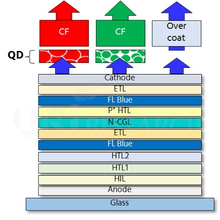
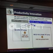
 

  1. Samsung OLED TV

At present, the TV industry trend is moving to OLED from LCD. Accordingly, Samsung Display is continuing research to resume their large area OLED for TV panel business. It is analyzed that Samsung Display possesses RGB OLED technology that uses SMS evaporation method, white OLED, and solution process OLED technology. However, as each technology has its drawbacks, they are carefully considering future directions. First, RGB OLED technology is estimated to lack Gen8 mother glass substrate evaporation equipment at present. Solution process OLED method has low material performance. For white OLED, as the key patents are owned by LG Display, technology that avoids these has to be first developed. Therefore, much attention is focused on which technology Samsung Display will use and invest in production line to enter the TV market.

[Merck Display Insight 2015] Merck Reveals Latest Performance Results for Red and Green Solution Process Materials

On November 5, during the 16th Merck Display Insight 2015 seminar, Merck revealed the development results for solution process materials. The solution process materials presented were red and blue materials’ efficiency, lifetime, and CIE.


At present UDC’s evaporation materials are being used in OLED mass production. UDC’s evaporation material performance, published on the company website, were compared with Merck’s materials. Merck’s red material’s efficiency was 19.1cd/A, lifetime was 5,900 hours, and the CIE was (0.66, 0.34) which were approximately 66% of UDC material’s efficiency (29cd/A), 26% of UDC material’s lifetime (23,000 hours), and showed equal CIE.


For Merck’s green material, efficiency was 76.4cd/A, lifetime was 5,200 hours, and the CIE was (0.32, 0.63). These were approximately 89% of UDC’s green’s 85cd/A of efficiency, and 29% of 18,000 hours of lifetime. The CIE were similar with UDC’s (0.31, 0.63).


The comparison of the published materials’ performance, efficiency of solution process materials are developed to the similar levels as evaporation materials, but material lifetime require more research. Through this seminar, Merck revealed that the LT95’s solution process material’s lifetime will be solution process OLED’s most crucial challenge.


During the question and answer part of the poster session, Merck also revealed positive outlook that full stack solution process OLED product will be produced within the next 3-4 years.


Despite being one of the latecomers within the OLED material business, Merck is producing notable results in solution process material development and OLED material sales. This year’s sales results are anticipated to be higher than expected.


According to 2015 Solution Process OLED Annual Report, published by UBI Research, the key issue for solution process OLED is solution process emitting material performance. The solution process red and green’s efficiency reached to the similar levels as evaporation material. However, lifetime showed to be ≤approx. 30% of evaporation material in LT95. On the other hand, solution process blue is analyzed to be falling behind evaporation material in both lifetime and efficiency. As such, it is estimated that solution process OLED will be mass produced using the hybrid structure where red and green are formed through printing, and blue is formed through evaporation.

What is Solution Process OLED’s Key Issue?

In the 2015 Display Printed Electronics Seminar held in The K Hotel in Seoul on October 7, Dankook University’s Professor Byung Doo Chin and Korea Research Institute of Chemical Technology’s Dr. Jaemin Lee gave presentations. They discussed key issues of solution process OLED; Professor Chin examined technological issues of print OLED/PLED device while Dr. Lee discussed technology trend of solution process OLED device.


Professor Chin reported that of the materials being used in current solution process, red, and green progressed greatly in terms of efficiency and lifetime. However, he explained that as blue’s efficiency and lifetime are lower than the other 2 colors, unless these issues improve, white actualization, as well as blue actualization, is difficult and panel cannot properly perform.


Material research development can occur for evaporation OLED only through material synthesis and purification. However, for solution process OLED, turning the materials to ink has to be additionally considered. Dr. Lee announced that diverse collaboration are happening between material and ink related companies for these reasons.


In the seminar, Professor Chin and Dr. Lee agreed that the key to the solution process OLED development is material characteristics development. According to the solution process material traits presented by Sumitomo Chem. and DuPont, while red and green traits are fast catching up to ones used for evaporation OLED, this is not true for blue. Despite these disadvantages, solution process OLED is a key technology that can produce large area RGB OLED panel using Gen8, or higher, manufacturing equipment; continued research development of solution process technology is expected in future.

Portfolio Items