投稿

JDI Announces OLED Mass Production in 2018

Japan Display (JDI) officially announced OLED mass production. The press, including the Sankei Shimbun and the Nikkei, reported that on January 22 JDI revealed their plans to begin mass production of OLED panel to be used in smartphone from 2018.


JDI continued development with the aim of LTPS TFT and WRGB OLED technology applied high resolution AMOLED panel mass production for mobile device, and revealed the results through exhibitions in recent years.


In Display Innovation 2014 (FPD International) and SID 2015, JDI have presented 5.2 inch FHD flexible AMOLED panel. Particularly, in SID 2015, JDI showed a notepad equipped with flexible OLED panel.


JDI is likely to mass produce flexible AMOLED following the current mobile device market trend. Although the mass production technology was not mentioned, due to the client demands, it is estimated that either the RGB method, which is being used by LG Display and Samsung Display, or WRGB method, which is being developed by JDI, will be selected.


At present, only Samsung Display and LG Display can mass produce flexible AMOLED panel, but Chinese companies are fast in pursuit. There is much interest in how this JDI’s mass production announcement will affect the future OLED market.


JDI

OLED Frontier Forum’s 3rd Section Panel Discussion Summary

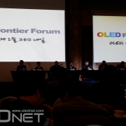
The 3rd section of the 1st OLED Frontier Forum (Jan 28), OLED’s Future, held a panel discussion with government, industry, and academia experts discussing OLED industry development strategy, such as next generation technology development, convergent areas, and personnel training, and future forecast. OLEDNET summarized the answers that each expert gave to the questions of the panel chair (Professor Changhee Lee, Seoul National University).


Jun-hyung Souk (Professor, Sungkyunkwan University)

For SDC mobile, as the OLED depreciation is ending the OLED production cost is becoming almost the same as LCD. If OLED related experts stay within Korean industry as well as the technology, Korea can continue to lead for 4-5 years. In order to achieve the continued leadership, differentiation through flexible R2R has to be carried out, as well as the materials and encapsulation technology development.


Sung-Chul Kim (CTO, SDC)

As a-Si is an existing technology, there is no room for further advancement. Sharp’s difficulty in panel business is due to lack of technology research on the panel. Because one technology can only be used for approximately 7 months, diverse technology development is required.


In-byeong Kang (CTO, LGD)

Fast organizations cannot but win. Therefore, rapid change to OLED from LCD is needed. As difficult is the technology, cooperation between academia and industry is needed. Now is the time when this cooperation for next generation technology development is more in demand. LGD is putting in much effort for OLED profitability.


Sung-Jin Kim (Vice President, Toray Advanced Materials Korea)

Cooperation between materials and manufacturing equipment companies is important in solution process materials development. Particularly, how to control dry process is an important issue. Also, Kim expects the current solution process materials development to show tangible results in 3-5 years.


Junyeob Lee (Professor, Sungkyunkwan University)

Solution process is favorable for materials optimization. From the initial concentration on polymer materials, recently small molecule materials focused soluble materials development is being carried out, and how to implement common layer is an issue. Emitting layer is using the small molecule materials that are being used as evaporation materials. The difference is the higher cost as the solvent is used. Also, as there is an issue (formulation problem) when used in large area, solution is required.


Kyoung-Soo Kim (Vice President, Korea Display Industry Association)

Expert acquirement is a key issue. Through upgraded cooperation between industry and academia, and industries, cooperation between panel, manufacturing equipment, and materials has to progress into a positive cycle. Also the open platform regarding new OLED application is needed.


Young-Ho Park (PD, Korea Evaluation Institute of Industrial Technology)

Flexible display competitiveness acquirement is a big concern. Programs for challenging R&D, and high added value product/technology development, and R&D infra establishment (highly cost-effective R&D) have to be considered.


패널토론회

Sung-Chul Kim, Samsung Display’s CTO, What is Needed for OLED To Enter New Areas?

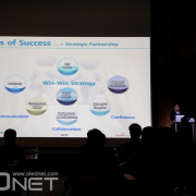
Sung-Chul Kim, Samsung Display’s CTO, at the 1st OLED Frontier Forum (Jan 28) gave a presentation ‘AMOLED Technical Issue and Future’ and discussed OLED technological issues of the past and present.


Kim pointed out the fact that glass substrate is not always necessary for OLED as the most different factor compared to LCD, and emphasized flexible OLED where plastic substrate is used. Kim reported that flexible OLED issues include window’s durability and coating, touch panel’s electrode materials and flexibility, reduction of number of encapsulation layers and flexibility, and backplane’s low stress structure and OTFT application. He revealed that developing spherical stretchable display, which the user can zoom in, is also included in the product roadmap.


Regarding transparent/mirror display, Kim announced that this is the direction that OLED should head toward and added that layout design development suitable for different application areas is needed. Specifically, the transparent display should be developed to increase the transmittance area and decrease the TFT area, and the mirror display to optimize the ratio between the total reflection and half-reflection areas.


Additionally, in order to produce high resolution OLED, Kim mentioned that innovation in terms of pixel operation and backplane structure is needed. He emphasized compensation circuit and that whether high resolution display can be manufactured cheaply and using simple structure is the key.


Kim discussed wall display, IoT, educational display, etc. as the new applications which will become important in future. Particularly, mentioning the automotive display area, Kim explained that for OLED to enter these new areas, plastic materials suitable for each applications and technology that can correctly process this are required. In order for this type of research development to be carried out smoothly, Kim added that cooperation between the academia and industry is necessary.


삼성기사

[Lighting Japan 2016] Yamagata University Develops Low Cost Flexible OLED Encapsulation

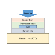
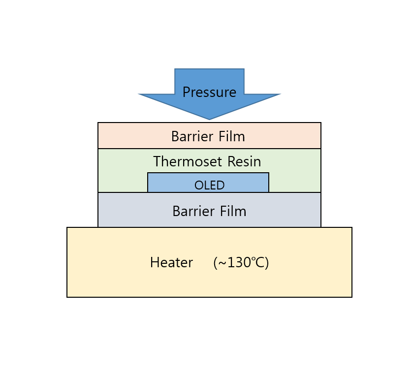
Innovation Center for Organic Electronics in Yamagata University in Japan discussed low cost flexible OLED encapsulation in Lighting Japan 2016 conference. Existing flexible OLED encapsulation mainly used hybrid encapsulation structure that forms multi-layer thin film passivation layers on top of OLED, and then applying adhesive organic material and laminating gas barrier film. The encapsulation structure presented by Yamagata University forms, of the hybrid encapsulation structure, thermoset resin and barrier film above OLED without multi-layer thin film passivation, and laminate at approximately 130 °C. Yamagata University announced that they were successful in transparent flexible OLED panel development on January 13 using encapsulation, and that this panel will be presented in Printable Electronics 2016 in Tokyo from January 27.


The OLED panel to be exhibited is a leaf shaped of 45 mm width, 110 mm length, weighs less than 1.2g, and 250 um thick transparent film substrate that can be folded.


According to Yamagata University, if the newly developed encapsulation is applied, the OLED lighting panel price can be reduced as passivation layer is not used. Also, Yamagata University revealed as it can satisfy both transparent and flexible categories simultaneously, it is estimated that it will become a key technology in future transparent flexible OLED lighting development.


Low Cost Flexible OLED Encapsulation, Yamagata University

Low Cost Flexible OLED Encapsulation, Yamagata University

[CES 2016] Big Changes in LG Display

On January 6 (local time), LG Display held a press conference with key board members in attendance including CEO Sang-Beom Han, CTO In-Byeong Kang, and head of marketing Young-Kwon Song.


lgd1


At this conference, unlike previously, Han conveyed strong determination and announced LG Display will invest in future large area display with OLED. This was a conviction never seen before.


The evidence of the confidence could be read at the exclusive exhibition. OLED TV achieved 800 nit, 150% higher than UHD Alliance’s standard of 540 nit.


lgd2


With transparent OLED, LG Display reached leading specs. The WRGB OLED structured transparent OLED has 40% transmittance and 600 nit of brightness through the application of the 800 nit OLED technology.


lgd3


Flexible OLED also was significantly different from last year. In 2015, the comparison between LG’s OLED and LCD for automotive dashboard display showed OLED to be lacking in brightness. However, this year’s exhibition showed OLED panel to have similar level of brightness as LCD and exceeding LCD’s spec with deeper black.


lgd4


The exhibition showed rapid development of LG Display’s OLED technology.

[2015 OLED Evaluation Seminar] Professor Hong Mun-Pyo of Korea University Retraces Flexible OLED’s Key Issues

By Hyun Jun Jang


During the 2015 OLED Evaluation Seminar (December 4) hosted by UBI Research, Professor Hong Mun-Pyo of Korea University gave a talk titled Flexible AMOLED Gas Barrier Technology Development Status. Through this presentation, he discussed in detail flexible OLED’s outline, technological issues, and encapsulation among other key issues.


Flexible display signifies a display that was produced on top of flexible substrate, and not an existing glass substrate, which can bend, fold, or roll without breaking. Hong emphasized flexible display is the next generation display that can simultaneously satisfy consumers and panel makers, and an area that OLED can be more valuable compared to LCD.


There are 3 essential issues in flexible display, substrate, TFT array, and display processes, as well as ancillary issues such as application and cost. Hong reported key issues regarding substrate and display process.


Flexible display uses plastic substrate, instead of glass, that is strong against shock and can bend. Therefore, handling technology that manages plastic substrate is considered a key technology in flexible display production. Hong revealed that for handling technology, a film lamination method and vanish coating method are mainly used. A film lamination method is where plastic substrate is attached to carrier glass using adhesive before being processed and a vanish coating method is where the PI substrate is coated to the carrier glass before processing. He emphasized that no matter which method is used, the debonding technology used to detach the plastic substrate from the glass plays a crucial role in deciding yield.


Hong followed the substrate discussion with encapsulation technology. Encapsulation technology prevents moisture and oxygen that affect OLED panel’s performance from infiltrating in order to increase the display’s lifetime. As it is a core process that decides OLED panel’s yield, OLED panel production companies are focusing on optimum encapsulation technology development.


Key issues of encapsulation technology that is currently being applied to flexible OLED, barrier coating related issues are considered the most important. Barrier coating is the coating applied to the plastic substrate to overcome the limitations that occur as existing glass substrate is replaced by plastic. For flexible encapsulation, as can type or frit seal technologies that were used for glass encapsulation cannot be used, face seal or TFE technologies that can be applied to flexible are used. Also, as the permeability of oxygen and moisture has to be 10-6g/m2day or less, high performing barrier coating technology is needed.


When barrier coating is used to flexible OLED, generally 3 problems occur. Firstly, physically cracks or particles can develop. Regarding this, Hong explained that this issue can be solved if process is properly maintained. The second problem is micro defects that can arise on the surface of plastic film, which can be solved through optimized process, according to Hong. Lastly, nano-sized pin holes can come up. Hong revealed that multi-layers of barrier coating can solve this problem.


Generally, when OLED panel is produced the thickness of encapsulation layer is not a big issue. However, Hong emphasized that the thickness becomes a core issue when producing flexible OLED panel. He reported that hybrid structure of encapsulation where gas barrier cover plate is attached to passivation layer placed via PECVD can be the solution.


Although the most suitable process technology for hybrid encapsulation production is R2R, as appropriate results are not obtained when CVD is applied to R2R, Hong reported that research is being carried out toward the sputtering using direction. He revealed that if reflection plate is added to the sputtering equipment and neutron beam release is induced, defects that occur during the sputtering process can be reduced as the target thin film stabilizes.


홍문표 교수2

[2015 OLED Evaluation Seminar] How can OLED Emitting Materials, Components and Other Materials Markets Survive?

By Choong Hoon Yi


At 2015 OLED Evaluation Seminar (December 4) hosted by UBI Research, Sung-Kee Kang, DS Hi-Metal’s CSO, reported that OLED display market has to expand through OLED TV and new applications in order for OLED emitting materials companies to grow.


Presenting under the title of ‘OLED Organic Material Technology, Industry Trend’, Kang introduced the current OLED emitting material value chain. He explained that within OLED emitting materials market, there are too many players considering the current volume and overall OLED display market expansion is a necessity. However, he added that for OLED display to compete against LCD display, OLED TV market has to expand successfully, and new application that utilizes OLED’s characteristics is needed.


In order to expand the market, development of OLED emitting materials and other materials is urgently in demand that meet the required conditions. Kang emphasized that at present new technology seeds promotion for the next OLED is needed as well as development of OLED emitting materials, and other flexible/transparent related materials with new functions.


Considering LG’s active OLED TV marketing, Apple’s interest in OLED panel application, and possibility for Samsung to apply AMOLED to all models among others, OLED market is anticipated to rapidly grow. Together with this, the industries of OLED emitting material and component/other materials with new functions are also expected to considerably grow.

Minus Growth for H1 OLED Material Market with Mere US$ 564 Million*

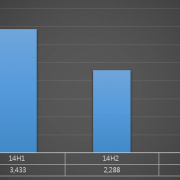
According to UBI Research, the 2015 H1 OLED material market recorded approximately US$ 564 million; this is a 14% increase compared to 2014 H2, but a 24% decrease against 2014 H1.


Despite reports that Samsung Electronics and LG Electronics are selling much larger volumes of flexible OLED applied Galaxy S6 Edge and OLED TV respectively compared to last year, the OLED material market is gradually stagnating.


The main reason for this OLED material market’s downward turn is Samsung Display’s operation level which remained stationary at 50% in H1. This led to stationary material usage compared to the year before. LG Display is producing flexible OLED and large size OLED panel for TV. However, approximately only 100,000 units of OLED panels were sold in H1 and material usage was also lowl. The current capa. is 34K but as the OLED material cost spent in H1 is approximately US$ 36 million, the operation rate is analyzed to be only 30% of the total capa.


The OLED material market is decreasing because the supply price is rapidly falling without increase in production volume. OLED material companies are frustrated at the 10-15% price decrease per quarter. At present, as the only clients are Samsung Display and LG Display, material companies are compelled to reduce the price as the failure to do so could lead toward the termination of business. OLED material companies spend several thousands of millions of dollars annually on development to meet constant improvement demanded by clients. There is much difficulty for OLED material companies as display companies continue with one-sided demands without compensation regarding development cost.


For OLED industry to maintain its continued growth, it requires more than success of panel companies. Material companies that play a pivotal part within the industry have to continue development and production of quality materials in order to create a healthy growth cycle. However, display companies are destroying the ecosystem.


What OLED material companies currently crave is for Chinese display companies to mass produce OLED panels as soon as possible.


* 1 USD = 1,100 KRW


OLED Material Market Revenue 2014 H1 – 2015 H1

OLED Material Market Revenue 2014 H1 – 2015 H1

[IFA 2015] The Return of the OLED King

Samsung Electronics, the current global leader of smartphone market share, challenged Apple to dominate smartwatch market with Galaxy Gear 2 armed with latest functions.


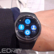
The exterior of Gear 2 changed to round type. Previous Gear copied rectangular fashion watch, but Gear 2 returned to the classic design.


Galaxy Gear2, IFA 2015

Galaxy Gear 2, IFA 2015


Gear 2 has the most basic circular shape, but the rotating bezel within the simple design boasts the perfect blend of digital and analog. The rotating bezel design used in stop watch in quality sports watch was applied to add a touch of analog. At the same time, the smartwatch has the digital side from the jog dial used in quality vehicles, merging the analog with digital.


Smartwatches until now had to be touched to change screen. However, Gear 2’s rotating bezel allows the screens to be changed easily through dial rotation.


Galaxy Gear 2, IFA 2015

Galaxy Gear 2, IFA 2015


Gear 2 applied flexible OLED produced by Samsung Display same as Gear with its 1.2inch size and 360×360 resolution. Compared to competitors’ 1.3inch, it might feel smaller but has the highest resolution; Samsung Electronics used a smaller display with better expressiveness. Particularly, absolute black, one of the advantages of OLED, is actualized with this product. The quality of black in previous Gear fell short and the screen wallpaper showed hints of blue. The new display shows that it is of OLED leader, Samsung family, with its brilliant colors using latest OLED materials.


Gear 2 also uses Tizen OS and firmly differentiated itself from other products. In fact, other products employed Google OS and had a problem of basically being the same under the different exterior leading to no particular differentiation factors for the consumers.


However, deserving the title of the leader of the smart device, Samsung Electronics utilized independently developed Tizen and boasted totally different interior.


Galaxy Gear 2, IFA 2015

Galaxy Gear 2, IFA 2015


Samsung Electronics is investing much effort in Gear 2 promotion; with the exclusive booth, visitors can examine diverse forms of Gear 2.


Galaxy Gear2 Booth, IFA 2015

Galaxy Gear2 Booth, IFA 2015

Attention Focused on Silver Nanowire as Key Material for Display

At IPEC 2015 (International Printed Electronic Conference), held on September 1, Professor Sang-Ho Kim of Kongju National University announced that silver nanowire technology is in initial stages of commercialization and will become display market’s key material.


Kim reported that when the bending radius of flexible display is reduced, 2 key issues occur with silver nanowire used as TSP (touch screen panel) material. First, the wiring that are crossed when bending is loosened as can be seen in figure 1. Due to this effect the bending stability decreases.

Fig. 1, Source: Professor Sang-Ho Kim, IPEC 2015

Fig. 1, Source: Professor Sang-Ho Kim, IPEC 2015


Kim explained that this effect can be solved by welding the two wires as shown in figure 2 using thermal annealing technology, laser process, and IPL photo-sintering technology.


Fig 2, Source: Professor Sang-Ho Kim, IPEC 2015

Fig 2, Source: Professor Sang-Ho Kim, IPEC 2015


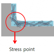
Another issue is a decrease in contact stability between nanowires at stress points when bending radius is reduced as shown in figure 3.


Fig 3, Source: Professor Sang-Ho Kim, IPEC 2015

Fig 3, Source: Professor Sang-Ho Kim, IPEC 2015


During the presentation, Kim explained that this can be solved through undercoating process. This process involves mixing 2 polymers with different Tg (glass-transition temperature) and layering it as in figure 4, and placing TSP on top.


Fig 4, Source: Professor Sang-Ho Kim, IPEC 2015

Fig 4, Source: Professor Sang-Ho Kim, IPEC 2015


Silver nanowire has benefit of being more flexible and less resistant compared to transparent electrode material, ITO. As such, it was spotlighted as TSP material most suitable for flexible OLED. Nonetheless, silver nanowire has been considered to fall behind ITO in panel mass production unit cost in display market.


However, haze effect which happens when sunlight is reflected off the silver nanowire TSP has been solved recently, and new touch technology that requires improved TSP functions, such as post-touch technology, has been developed. Accordingly, products that use silver nanowire are increasing despite the unit cost difference.


Kim reported that as TSP sheet resistance can be reduced through undercoating and welding technology and greatly increase bending stability, it is estimated that silver nanowire’s marketability will grow for flexible display.