Planar Aims for Transparent OLED Product Mass Production in Feb 2016
On November 30 (local time), a US based display production company Planar held an online presentation titled ‘Planar Look Thru OLED Transparent Display Webinar’, discussing transparent display traits and disclosing specifications for products which are estimated to be mass produced from February 2016.
Transparent display is defined as a display with see-through screen showing objects behind the display as well as the display contents. Recently, it is receiving much attention as a technology with high potential for diverse applications expanding existing display industry.
Planar explained that unlike the existing display, transparent display pixels are separated into transparent and emitting areas with RGB subpixels located in the emitting area. Planar clarified that what is black on general display becomes see-through and white becomes opaque.
Transparent display’s performance is decided by several factors such as transmittance, brightness, and color gamut. Regarding this, Planar revealed that the transmittance of transparent display is not fixed but can be affected by ambient light; brighter the surrounding environment, higher the transmittance. Additionally, viewers have tendency to perceive the display with higher color gamut as brighter than the actual brightness, and transparent display’s color gamut is therefore an important factor.
In early 2015, Planar revealed a 55inch transparent OLED display prototype. At present, Planar is receiving pre-order and aiming for mass production in February 2016. The company also reported basic specifications for the panel: 45% of transmittance, 100% color gamut, and Full HD (1,920×1,080) of resolution. The product also has 5 input sources: 4 HDMI terminals, and 1 display port.
During the webinar, Planar explained that 32 touch points using IR (infra-red) touch system installation is an option. Although this is less accurate than touch system using touch film, Planar explained that this was an unavoidable choice in order to increase the transmittance. They also added that they are continuing research for new touch system application.
The 55inch panel price starts from under USD 15,000 and Planar is currently receiving pre-order. Although there are many factors that affect transparent OLED’s lifetime, it was measured to be 20,000 hours at LT50. Answering the question on whether it is affected by UV light, Planar explained that it can be UV sensitive and the product was designed to be an indoor installation.
It is estimated that the transparent OLED panel used in the Planar’s product released is produced by Samsung Display as it has the same 45% transmittance, 1920×1080 resolution, and 400nit brightness.

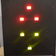
Planar’s Transparent OLED Display to be Mass Produced Source: Planar