Korea’s Last PMOLED Company to Fade into History?

NeoView Kolon, a subsidiary merged by Kolon Group in order to foster electronics business in 2001, is known within the industry to close down the PMOLED sector on December 31.


NeoView Kolon established factory in Hongseong, South Chungcheong Province of South Korea in 2003 and began PMOLED mass production. At this point, Samsung SMD (the current Samsung Display) and LG Electronics were also mass producing PMOLED. Other PMOLED producing companies included Korea’s Orion, Japan’s Futaba, and Tohoku Pioneer, and China’s Visionox. However, Samsung SMD stopped PMOLED business and sold manufacturing equipment to China’s Truly, and Samsung Display began AMOLED business from 2007. Subsequently, LG Electronics also closed down PMOLED sector and merged OLED related personnel to LG Display and launched AMOLED business. Orion was sold to China’s Changhong.


With the active application of AMOLED to Samsung Electronics’ Galaxy series, global PMOLED business began to rapidly shrink, and in order to maintain business, PMOLED companies pushed ahead with OLED lighting panel business.


NeoView Kolon entered into the automotive instrument panel business with PMOLED transparent display, but this business was also not easy. Furthermore, as the factory location is Hongseong, deep in the countryside, there was high turnover of employees and difficulty in technology development and recruitment. Despite the investment of over 100,000 million KRW, the company showed continued deficit.


NeoView Kolon turned into a financial sinkhole for Kolon Group and worsened the Group’s financial structure, leading to persistent discussion of selling or withdrawal of the business. Recently, Samsung Display is actively pushing forward the transparent AMOLED panel business. As such, transparent display business value for Kolon decreased, and it is estimated that this led to the decision of closing down the business.

New Products to be Released Using Visionox’s AMOLED Display

On Dec. 25th, Visionox announced that two products using its display panels will soon be released, including a 5.5 inch AMOLED display applied to high-end smartphone, and a 1.45 inch AMOLED display applied to smartwatch.


5.5 inch AMOLED Display Panel, Source : Visionox

5.5 inch AMOLED Display Panel, Source : Visionox


It is noted that the 1.45 inch AMOLED display has a display resolution of 272X340 and pixel resolution of 300 ppi, which reaches the highest pixel resolution in the domestic similar products. The thickness is less than 1 mm and the frame is only 1.5 mm. Furthermore, this display also offers MIPI and SPI interface functionality.


1.45 inch AMOLED Display Panel, Source : Visionox

1.45 inch AMOLED Display Panel, Source : Visionox


The smartwatch using 1.45 AMOLED display will be on sale in mainland China during the Spring Festival 2016 and the smartphone using 5.5 AMOLED display will be released to overseas market in Mar. 2016

Transparent Electrode Needs Development for Next Generation Display to Surge

Recently, with various research results regarding transparent electrode, interest in next generation transparent electrode is increasing.


In early December, UNIST (Ulsan National Institute of Science and Technology) developed printing technology that can arrange the Ag nanowire in the direction chosen on top of substrate. Ag nanowire is transparent electrode that can be applied to large area flexible touch panel and display products. This technology allows the surface to be flat through the fusion of nanotechnology to the existing printing process and increases transmittance.


Around the same time, ETRI (Electronics and Telecommunications Research Institute) developed technology that replaces thin metal electrode on top of OLED substrate with graphene transparent electrode. The metal electrode that were being used in OLED was mostly silver (Ag) material, but due to the reflection of internal light, the viewing angle changed depending on the angle. The external light also affected picture quality due to reflection. The newly developed technology used graphene that mostly does not reflect internal/external light as transparent electrode and improved transmittance and picture quality.


At present, ITO (indium tin oxide) is most widely used as transparent electrode materials. However, the supply is limited and flexible electronic device application is narrow. As such, the demand for the development of new materials that can replace this is greatly increasing. Particularly, as ITO is not suitable for stretchable device, the next generation transparent electrode development is considered to be a key issue for future display.


At 2016 Production/Process Technology Development and Application Cases by Flexible Transparent Electrode and Film Materials Seminar (December 17) held in Seoul, South Korea, Dr. Won Mok Kim of KIST (Korea Institute of Science and Technology) discussed, of many flexible transparent electrodes, TCO (transparent conductive oxide) production and process technology through presentation titled ‘TCO based flexible transparent electrode production and process technology development trend and applications’.


Of the transparent conductive materials, oxides have been researched the longest, and they are most widely used transparent conductive materials. Oxide including conductive materials have optical band gap of ≥3.0 eV and therefore has high transmittance and can be flexible. Kim revealed that TCO needs further improvement in conductivity and transmittance for display application.


Regarding transparent body, when refractive indexes of components are different, the path of light through the transparent body is refracted. When this occurs, the object becomes hazy although transparent. Haze is quantified and used to assess the transparent body’s performance. Kim explained that for solar cell the haze is purposefully increased to transmit more light to the internal active materials. However, if the display is clouded the clarity of image is reduced and therefore haze has to be lowered. To achieve this, Kim reported that the TCO’s surface roughness has to be reduced.


Kim revealed that there are two issues, temperature and flexibility, when TCO is used as transparent electrode. ITO’s conductivity is highest at 300 ℃, and for ZnO it is around 200 ℃. Channel cracks could occur with TCO when higher than bending strain is applied, and the crack could snap when it is bent further, destroying the device performance. Kim explained that to increase the bending strain, the thickness has to be reduced. However, when doing so as the sheet tension increases, the process has to be designed carefully considering the tradeoff.


Transparent electrode could be applied to display, solar cell, touch panel, and lighting among others and therefore requires much development. Although oxides have been long researched as transparent electrode materials, Kim concluded that even more diverse value can be created through fusion with next generation materials.


그림1

OLED and Graphene Together Achieves Innovative Technology

By Choong Hoon Yi


Korean research team is expected to greatly improve display’s transmittance and picture quality through fusing graphene technology, focus of much attention as the new material to OLED technology.


On December 15, ETRI (Electronics and Telecommunications Research Institute) replaced the thin metal electrode that was used as transparent electrode on top of the OLED substrate with graphene transparent electrode, and succeeded in developing original technology that is conductive and transparent.


This research results were presented in Scientific Reports, a journal from the publishers of Nature on December 2.


The metal electrode used in OLED until now has been mostly silver material, but due to the reflection of internal light, the viewing angle changed depending on the angle. The external light also affected picture quality due to reflection.


In order to solve this problem, ETRI research team focused on graphene that mostly does not reflect internal/external light. By replacing the material, the team reported that the transmittance increased by approximately 40% and reflectance improved by approximately 60%.


OLED was successfully lighted by attaching graphene transparent electrode to the organic layer on top of the film form (23 x 23 mm, 30 ㎛ thickness) of substrate. The research team believes this will be able to contribute much when applied to transparent OLED display and white OLED-based large area OLED display in future.


Particularly, unlike the existing vacuum process OLED production method, this technology can be employed via lamination where film is attached to the organic layer and graphene. Therefore, OLED can be produced through simpler process. It is expected that this can be evolved into production technology using roll to roll process.


Additionally, ETRI, together with Hanwha Techwin, is working on applying graphene transparent electrode to OLED’s lower electrode through collaboration of high quality graphene thin film electrode materials. The related technology development results were published online by The IEEE (Institute of Electrical and Electronics Engineers) of Selected Topics in Quantum Electronics.


ETRI’s Dr. Jeong-Ik Lee (soft I/O interface research section) anticipated that “this technology will be able to play a role in widening the gap with latecomer countries in OLED industry where challenging latecomers are strong”.


This research was carried out through Korea’s Ministry of Science, ICT and Future Planning and Institute for Information & Communications Technology Promotion (IITP)’s “Energy reducing environment adapting I/O platform technology development for future advertisement service” project and Ministry of Trade, Industry and Energy and Korea Evaluation Institute of Industrial Technology’s “Substrate size 5.5 generation or larger graphene film and OLED device/panel foundation and application technology development for graphene materials OLED transparent electrode and thin film encapsulation application”.


ETRI is planning to additionally develop sheet tension reducing technology by manufacturing metal in thin, grid forms and enlargement technology to produce mobile display size within 2016.


Through this technology, the research team produced 6 international patent applications and 6 papers. ETRI is intending to transfer the technology to graphene film and display panel companies among others. Commercialization is estimated to begin after 3 years.

1.Graphene transparent electrode applied lit OLED

1. Graphene transparent electrode applied lit OLED


2. OLED with existing thin metal electrode and graphene electrode OLED comparison (Left: Graphene, Right: Thin Metal, Ag)

2. OLED with existing thin metal electrode and graphene electrode OLED comparison (Left: Graphene, Right: Thin Metal, Ag)


3.Film including graphene transparent electrode applied to lamination process using OLED production

3. Comparison graph of existing thin metal electrode OLED and graphene electrode OLED


4.Film including graphene transparent electrode applied to lamination process using OLED production

4. Film including graphene transparent electrode applied to lamination process using OLED production


5.Graphene transparent electrode OLED Production Process

5. Graphene transparent electrode OLED Production Process


[Process Explanation]

After manufacturing laminated film, formed with bonding layer (BL) and PET film, using surface treated substrate, graphene transparent electrode is transferred on to the bonding layer. By laminating the laminated film that includes graphene transparent electrode on the substrate (lower electrode and organic layer), OLED where graphene transparent electrode is used as upper electrode is complete.


6.Graphene OLED of diverse colors

6. Graphene OLED of diverse colors

Now is the Time to Invest for OLED to be the Next Generation Display

By Hyun Jun Jang


이창희


On December 10, a seminar specializing company bizocean held ‘2016 Next Generation Display’s Latest Trend and Cutting Edge Industry Application Issues and Business Creation Seminar’ in Korea Technology Center. Professor Changhee Lee of Seoul National University, the first speaker of the seminar, announced that as OLED will become the technology for future display, now is the time for investment by the companies.


Lee reported that the display follows camera’s resolution, and although resolution has been developed up to UHD, he forecast that it will advance further. He also added that higher the resolution, the display performance that consumers demand will increase.


Regarding the current display market status, Lee explained that as the LCD’s margin is falling the market has to turn to OLED, but it is still expensive and capacity is low. Additionally, from the way consumers are still using the term liquid crystal regarding Samsung’s AMOLED smartphone, Lee speculated that people have difficulty in distinguishing between LCD and OLED. He told the audience that the industry should inform the public of the OLED’s differences from LCD through transparent, flexible displays that show OLED’s superior traits, and open the market through product differentiation strategy.


For the future display, Lee pointed out printing OLED. He explained that although printing OLED’s lifetime, particularly blue’s, falls short compared to vacuum evaporation, it is estimated to reach commercialization stage after 2-3 years. Despite the flaws in terms of materials, Lee reported that the advantages such as reduced production cost, fast tact time, and material usage efficiency will lead to the opening of the market. For these reasons, Samsung and LG are carrying out development.


Lee forecast that LCD, in its maturity stage of the industry life cycle, will lead the market for a while, but OLED technology will rapidly evolve and become the focus of the next generation display market. Regarding OLED TV, Lee mentioned that large area OLED mass production through printing technology is urgent in order to achieve price competitiveness. At present, OLED’s capacity is less than 1/100 of LCD. As such, even if there is demand, supply may not be able to meet it and Lee suggested the need for investment to the companies. He added that if there is low supply when the number of customers is high, the opening of the market could be delayed.


이창희2

Display Market Forecast Source: Professor Changhee Lee Presentation Material


Lee mentioned QLED as another future display technology. QLED has the same structure as OLED but uses quantum dot as the emitting materials, changing colors through different sizes. Lee reported that the color gamut is high as the wavelengths are shorter than OLED emitting materials. Also as the same material is used, QLED has an advantage of reduced material production cost and development of micro display with 2,000 ppi is complete. However, Lee added that as the lifetime is nowhere near sufficient, commercialization stage is still far away.

[2015 OLED Evaluation Seminar] Oxide TFT Technology that 2015 should Spotlight

By Hyun Jun Jang


During the 2015 OLED Evaluation Seminar (December 4) hosted by UBI Research, Professor Jin-Seong Park of Hanyang University gave a presentation titled OLED Oxide TFT Technology Trend, discussing oxide TFT, related industry, and technological issues as well as TFT technology that should receive the spotlight in 2016.


Oxide TFT has an advantage of high mobility and large area uniformity compared to a-Si TFT. As such, it is being more applied to large area OLED panel and used in LG Display’s OLED TV.


Park revealed that there are mainly 4 issues regarding oxide TFT and led with the reliability issue. Oxide TFT is essentially in amorphous state but when crystalized, the density and crystallizability increase; as oxygen does not move away and stay in place, defects occur less and reliability is high. Japan’s SEL and Sharp published CAAC (C-Axis Aligned Crystal) structure related oxide TFT paper, and Cornell University produced CAAC oxide TFT by increasing the substrate temperature and adjusting oxygen’s partial pressure.


The second issue is composition ratio. Park reported that composition ratio is the most closely related characteristic to TFT’s mobility. He revealed that recently research is being carried out centering around IGZO (indium gallium zinc oxide), but also oxide TFT research with different composition ratio is continually published. For example, ITZO (indium tin zinc oxide)’s mobility has been reported to reach 30cm/Vsec, and BOE is working on the related research. Research results, which showed increased mobility and reliability for IGZTO, which is IZTO with G added, was published, as well as ZnON (zinc oxide nitride) TFT’s 100cm/Vsec mobility. BOE demonstrated ZnO TFT applied 14.1inch AMOLED.


The third issue is the device structure. Park explained that efficiency can increase when top gate structure is used to oxide TFT as parasitic capacitor is not needed, but that the process is difficult. However, Park reported that JOLED revealed when self-alignment is used the number of masks used can be reduced and increases performance. This structure is applied to OLED TV by LG Display.


Lastly, Park gave the safety of device as the last issue. Oxide TFT can exhibit degradation effects from light, oxygen, hydrogen, and moisture. Park reported that hydrogen particularly has great effect on the safety. He explained that although the current prevailing OLED TFT is LTPS, as the panel becomes larger there will be technological competition between oxide and LTPS. Reporting that TFT which is cost efficient and shows high performance in diverse factors such as resolution will dominate the market, Park concluded his presentation.


박진성교수

[2015 OLED Evaluation Seminar] Professor Hong Mun-Pyo of Korea University Retraces Flexible OLED’s Key Issues

By Hyun Jun Jang


During the 2015 OLED Evaluation Seminar (December 4) hosted by UBI Research, Professor Hong Mun-Pyo of Korea University gave a talk titled Flexible AMOLED Gas Barrier Technology Development Status. Through this presentation, he discussed in detail flexible OLED’s outline, technological issues, and encapsulation among other key issues.


Flexible display signifies a display that was produced on top of flexible substrate, and not an existing glass substrate, which can bend, fold, or roll without breaking. Hong emphasized flexible display is the next generation display that can simultaneously satisfy consumers and panel makers, and an area that OLED can be more valuable compared to LCD.


There are 3 essential issues in flexible display, substrate, TFT array, and display processes, as well as ancillary issues such as application and cost. Hong reported key issues regarding substrate and display process.


Flexible display uses plastic substrate, instead of glass, that is strong against shock and can bend. Therefore, handling technology that manages plastic substrate is considered a key technology in flexible display production. Hong revealed that for handling technology, a film lamination method and vanish coating method are mainly used. A film lamination method is where plastic substrate is attached to carrier glass using adhesive before being processed and a vanish coating method is where the PI substrate is coated to the carrier glass before processing. He emphasized that no matter which method is used, the debonding technology used to detach the plastic substrate from the glass plays a crucial role in deciding yield.


Hong followed the substrate discussion with encapsulation technology. Encapsulation technology prevents moisture and oxygen that affect OLED panel’s performance from infiltrating in order to increase the display’s lifetime. As it is a core process that decides OLED panel’s yield, OLED panel production companies are focusing on optimum encapsulation technology development.


Key issues of encapsulation technology that is currently being applied to flexible OLED, barrier coating related issues are considered the most important. Barrier coating is the coating applied to the plastic substrate to overcome the limitations that occur as existing glass substrate is replaced by plastic. For flexible encapsulation, as can type or frit seal technologies that were used for glass encapsulation cannot be used, face seal or TFE technologies that can be applied to flexible are used. Also, as the permeability of oxygen and moisture has to be 10-6g/m2day or less, high performing barrier coating technology is needed.


When barrier coating is used to flexible OLED, generally 3 problems occur. Firstly, physically cracks or particles can develop. Regarding this, Hong explained that this issue can be solved if process is properly maintained. The second problem is micro defects that can arise on the surface of plastic film, which can be solved through optimized process, according to Hong. Lastly, nano-sized pin holes can come up. Hong revealed that multi-layers of barrier coating can solve this problem.


Generally, when OLED panel is produced the thickness of encapsulation layer is not a big issue. However, Hong emphasized that the thickness becomes a core issue when producing flexible OLED panel. He reported that hybrid structure of encapsulation where gas barrier cover plate is attached to passivation layer placed via PECVD can be the solution.


Although the most suitable process technology for hybrid encapsulation production is R2R, as appropriate results are not obtained when CVD is applied to R2R, Hong reported that research is being carried out toward the sputtering using direction. He revealed that if reflection plate is added to the sputtering equipment and neutron beam release is induced, defects that occur during the sputtering process can be reduced as the target thin film stabilizes.


홍문표 교수2

[2015 OLED Evaluation Seminar] Can LG Display and Samsung Display Become OLED Market’s Rule Maker?

By Hyun Jun Jang


At 2015 OLED Evaluation Seminar (December 4) hosted by UBI Research, UBI Research’s president Choong Hoon Yi gave a talk titled AMOLED Panel Industry Trend and Market Forecast discussing OLED industry until 2015 and forecasting 2016 OLED market.


Yi presented 2 issues related to flexible OLED. The first issues he discussed was regarding foldable types in foldable display. Yi explained that in-folding is where display is placed inside and out-folding has display on the outside, and revealed that in-folding type is mainly being developed. He also added that these technologies will be useful in FinTech (financial technology: new form of financial technology using mobile, social network, big data, etc.).


According to Yi, another issue for flexible display is film application. In order to increase the yield of flexible display, film has to replace cover glass. However, this could lead to unpleasant touch sensation and Yi emphasized technology such as polishing has to be applied to improve this to convince the consumers.


Regarding the market, Yi estimated that the total global smartphone market will grow to record approximately 2,000 million units until 2020, with Samsung Electronics’ 400 million units. He also estimated that the OLED display proportion of Samsung’s Galaxy series will continue to increase and that most of Galaxy products will have AMOLED panel in 2019. Of this, Yi announced that flexible OLED and rigid OLED are to record approximately 280 million units and 120 million units respectively. He also forecast that the OLED TV market will grow into approximately 11 million units and that materials and equipment companies will rapidly grow.


At present, the display market is entering low growth state, and companies are focusing on strengthening the market competitiveness through new technology development and production potential increase. Samsung Display is actively striving to increase OLED panel’s supply for external companies. LG Display announced 1.84 billion KRW investment for world’s largest OLED focused P10 factory and other areas.


Yi reported that as flexible OLED evolves, the mobile display resolution competition of the present will disappear, and he estimated that as LTPS-LCD market decreases, the sales of related panel companies, such as BOE, Sharp, JDI, and LGD, will diminish.


Yi also told the audience that he is expecting Samsung Electronics to put OLED TV on the market from 2018 and the sales of the companies, Sharp, AUO, and CSOT, that were supplying them with LCD panels will fall. Essentially, he explained that as the OLED market grows, LCD dealing companies’ position will weaken which will lead to the strengthening of OLED panel production and related companies’ position.


When asked about the future of Korean display panel companies, Yi replied that when LCD and OLED are competing, set companies decides the market. However, if OLED can unite the market, Yi emphasized that the display panel will be rebranded as Rule Maker and LG Display and Samsung Display will be in its center.


대표님

[2015 OLED Evaluation Seminar] Transparent Flexible Display’s Necessity Found in Worth

On December 4, UBI Research hosted 2015 OLED Evaluation Seminar in HJ Convention Center in Seoul, South Korea. The first speaker, LG Display TFD Biz Operation Group’s Chief Research Engineer Jeonghyun Kim spoke on transparent and flexible display’s worth.


Under the title of ‘Transparent/Flexible Display’s Future’, Kim discussed overall development trend of display and marketability. At present, the display market is changing to OLED, but as the growth rate is decreasing Kim added that new market creation is necessary. He explained that this is the time for a breakthrough of new market and transparent flexible display can play the lead. Kim also mentioned the marketability of transparent flexible display that can be actualized through OLED.


Transparent flexible OLED display possesses high technology level required by plastic substrate, low temperature process technology, and module among others. However, while introducing transparent and flexible OLED display’s worth, Kim emphasized the need for related technology development. The transparent display’s worth, mentioned by Kim, includes space expansion potential through home interior design, communication and safety increase within public facilities, AR information on existing transparent area, and sentimental and recreational experience at observatory and gallery. Regarding flexible display’s worth, he cited mobility in thinness and lightness, utilization through digital board, and space expansion through design freedom.


As a prime market for transparent flexible display application, Kim discussed automotive display market; considering the automotive market trend toward driverless/electric vehicles, display utilization inside the vehicle will increase and automotive industry will seek OLED display first.


With the LG Display’s video with diverse applications of transparent flexible display and future direction for display, Kim concluded his presentation.

[Expert Talk] Interview with SAES Group’s Dr. Mauro Riva

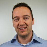
Dr. Mauro Riva, SAES Group’s OLED/OLET business developer, kindly answered a few questions regarding OLED for OLEDNET. He will be speaking at the 2nd OLED KOREA Conference (February 24-25, 2016) in Seoul, Korea.


With much thanks to Dr. Riva for taking the time to answer some questions, here is the full script of the interview.


  • What is your personal opinion on OLED’s marketability?

I believe that OLEDs have just to leverage on their unique, distinctive properties, in order to enable brand new market segments, rather than entering competition in already crowded and established markets. I mean that the specificities of organic materials make them the only candidates for creating an entire future portfolio of portable, flexible, feather-light and, possibly, low power high definition display devices.

Thus, the ability to generate really new, fancy, conformable and sustainable displays is, in my opinion, the first ingredient to boost OLED’s marketability. The second ingredient could be, in the long run, lower raw material and manufacturing costs, with respect to competing display technologies.


  • Is there a particular reason for your choice to speak at the OLED specific conference rather than a more general IT conference?

As an advanced materials Company, SAES Group have developed a comprehensive portfolio of functionalized polymer composites, to be integrated in a plurality of OLED device architectures. For this reason, an OLED specific conference is the perfect place to directly discuss the important theme of encapsulation, with the people working everyday on this peculiar technology. We wanted to have a direct and frank debate with scientists and technicians specifically involved in OLEDs, rather than in general IT themes, in order to be far more focused on the manifold organic diode encapsulation issues.


  • What are the latest issues on OLED encapsulation?

I think that OLEDs are nowadays facing the same issues they had since the beginning: basically, OLED materials are extremely sensitive to oxidizing agents and, especially, to moisture. This requires encapsulation materials with exceptionally high barrier properties, and active fillers or getters, capable of absorbing water on a single molecule basis. The optimization of many functional properties in single encapsulating materials is a very complex materials science problem. The fact that OLED materials can also be very sensitive to heat or radiations, generates many process constraints as well.

It turns out that encapsulation materials must be specifically engineered taking into account the OLED structure, the device architecture, the chemical and physical nature of the materials and, nevertheless, the specific processes to be applied. Perfecting OLED encapsulation is thus a very challenging task, which requires deep technical interaction between advanced encapsulation materials providers and OLED makers.


  • Could you tell me about development concept and characteristics? Also perhaps recent performances and outcome?

As far as the Organic Electronics Business Development Area is concerned, we provide a very large portfolio of active edge sealants, active transparent fillers, dispensable getters. These products come as the result of our deep know-how in functional polymer composites, and they are specially tailored to address customers’ specific OLED designs and processes. Leveraging on our functional polymer composite technology, we have been able to develop solventless formulations, with water sorption capacities exceeding 13 percent in weight and very high flexibility and adhesiveness for fully bendable devices. Our products can be applied via screen printing, blading, syringe, ink-jetting, ODF and even be employed in thin film encapsulation structures, to make them simpler and more reliable.

Together with the functional polymer composite based products, we also provide high performance tape dryers, as thin as 110 microns, for R&D and small scale bottom emission OLEDs. Another important class of products is related to AlkaMax: this technology offers an efficient and safe method of depositing ultrapure alkali metals. Our alkali metal dispensers and pills keep the alkali metal pure in the form of a stable salt, until it is thermally activated in the evaporation chamber.


  • What are OLED related main manufacturing equipment type and who are your main clients?

We see syringe dispensing as one of the main methods for dispensing our functional polymer composites. Ink-jetting is also becoming more and more widespread, together with ODF, especially for active fillers. As of today, we get the most revenues in this field from PMOLED makers. The AMOLED market is broadening, and we have some very good customers there as well, who are especially in need of effective solutions for smartphone and tablet size high definition displays. OLED lighting is still early stage, but we are already collaborating with the major players in that field, so far at R&D or pre-production stage. The main market for our products for the organic electronics market is indeed Asia.


  • Are there any areas where you are collaborating with material companies?

We have many collaborations worldwide, with other material companies as well. Regarding the functional polymer composite technology, we are collaborating in the areas of organic electronics, specialized food packaging and gas barrier films.

We are also engaged in very fruitful collaborations with specialized equipment makers.


  • Is there anything you would like to add?

I would just kindly invite everyone who is interested in OLED encapsulation to visit our website and to directly contact us, for deepening all the technical aspects about our product portfolio.

The proactive and collaborating approach with our customers and the Research and Innovation focus have always been the heart of our Company way of doing: the OLEDs world offers us a real exciting and challenging arena for making innovation happen, together with all the players involved in this fascinating emerging technology.